![[VerilogHDL] RISC-V 기본, RV32I R-Type, IL-Type](https://img1.daumcdn.net/thumb/R750x0/?scode=mtistory2&fname=https%3A%2F%2Fblog.kakaocdn.net%2Fdna%2Fc3nci9%2FbtsH3N4gbXr%2FAAAAAAAAAAAAAAAAAAAAAH58etEkdrqs0IPiMaslJNfU9KqV598CQZCQZeqfg-_4%2Fimg.png%3Fcredential%3DyqXZFxpELC7KVnFOS48ylbz2pIh7yKj8%26expires%3D1777561199%26allow_ip%3D%26allow_referer%3D%26signature%3DXU30GYsMeTxefy4Qt33JPs50aIQ%253D)

1. RISC-V


RV32I(Base Integer Instruction Set)를 구현해보자.
→ 곱셈, 나눗셈 연산이 없는 정수형 명령어 세트
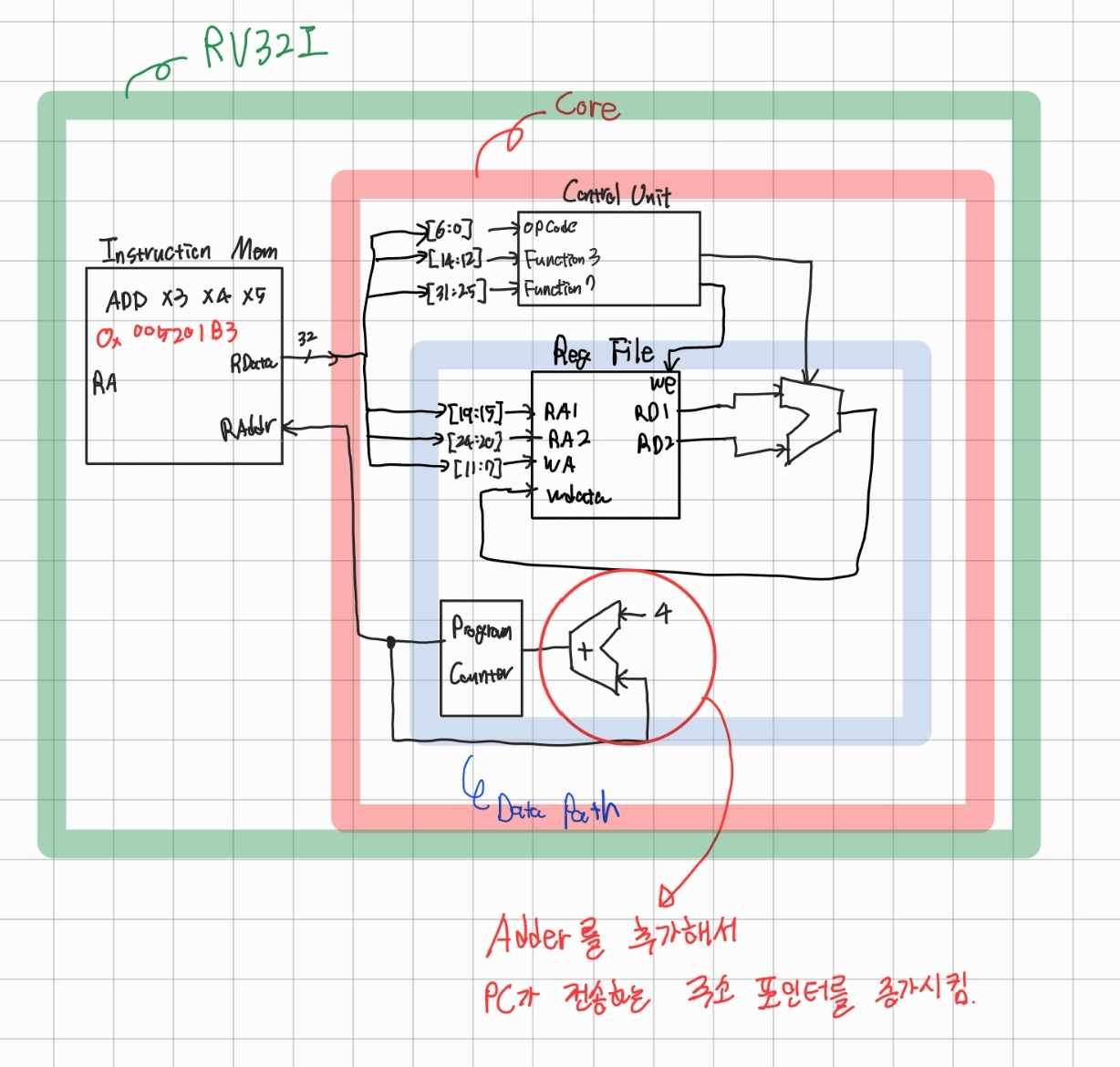
Instruction 구조

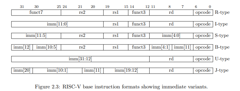
(1) : RV32I의 Register File : 32개의 레지스터
(2) : 명령어 구조는 32bit 고정(RISC의 특징), R ~ J-Type 구조가 있다.

각 명령어 레지스터에 대한 프로그래밍 권장사항(의미부여) → 굳이 안따라가도 되지만 이런식으로 가이드가 정해져있다.
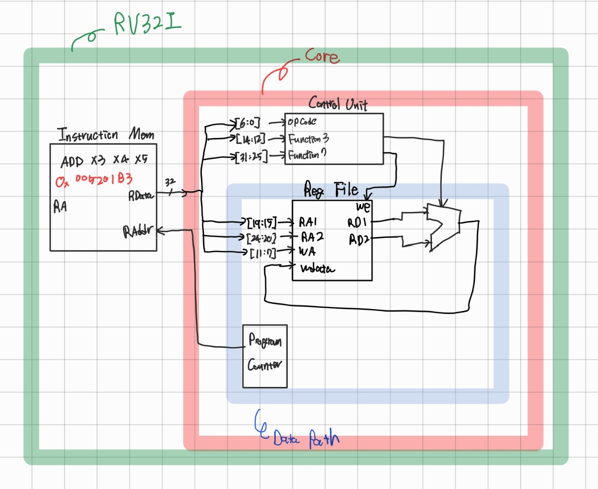
2. CPU 기본 모듈
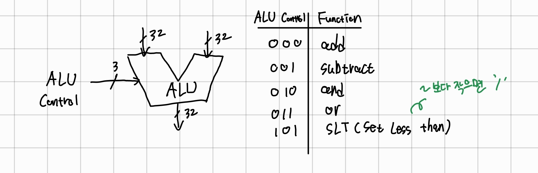
- ALU
- Register File
- PC(Program Counter) Register
- Instruction이 실행할 위치(Instruction Memory)를 가지고 있는 Register
- Instruction Memory
- Data Memory

3. RV32I R-Type Instruction
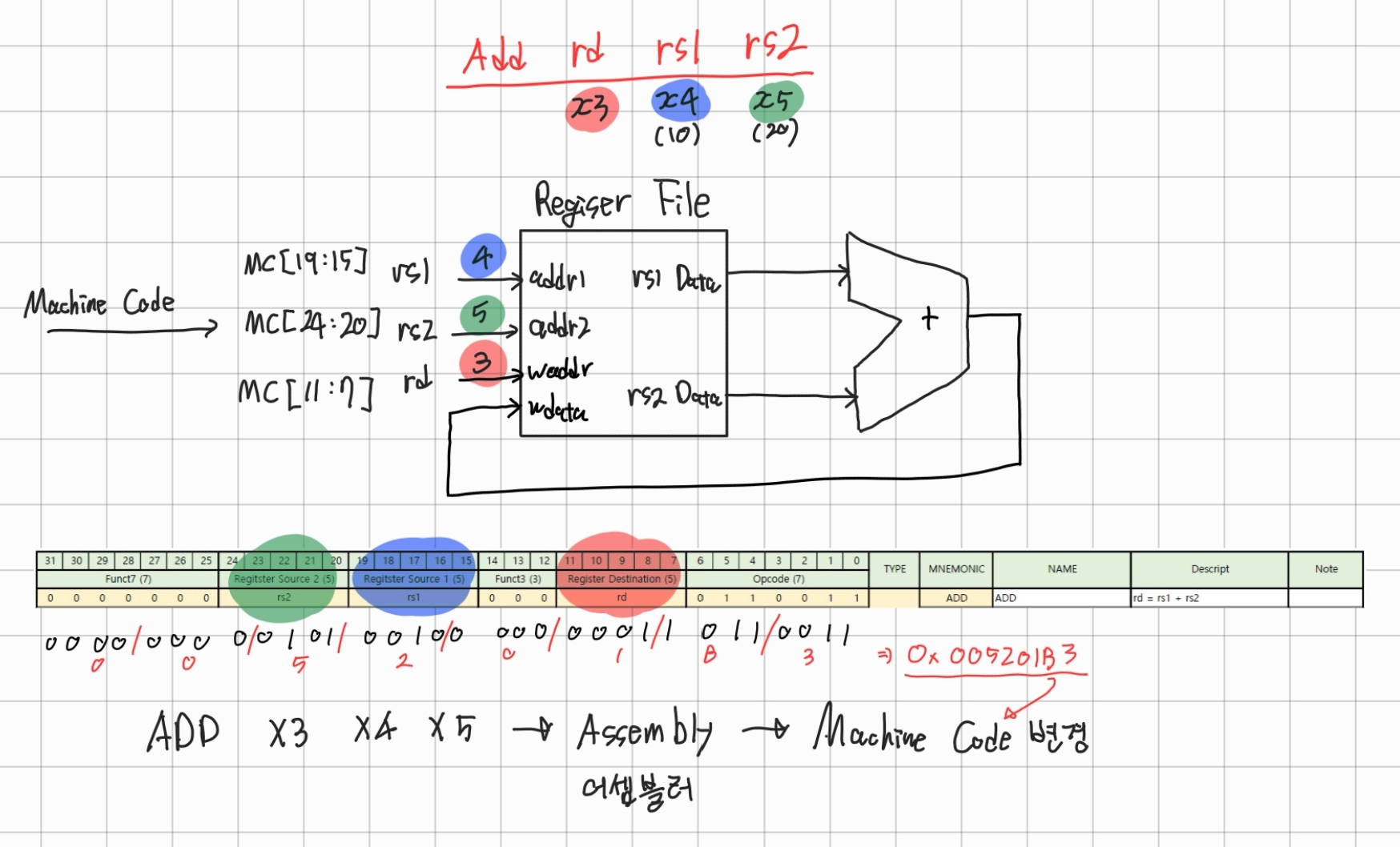
- Register File에 저장된 2개의 값을 연산하여 Register File에 저장

OP Code: Type을 나타내는 코드Funct7,Funct3: Type에서 어떤 연산을 할 것인가(ALU 동작)rd: 연산한 값을 저장할 주소rs: 연산할 소스 주소

구현
위 그림과 같이 구현해보자!!
Data Path 구현
`timescale 1ns / 1ps

module DataPath (
    input logic        clk,
    input logic        reset,
    input logic [31:0] machineCode,
    input logic        regFile_wr_en,
    input logic [ 2:0] ALUControl,

    output logic [31:0] instrMemRAddr
);

    wire [31:0] w_ALUResult, w_RegFileRData1, w_RegFileRData2;

    Register U_PC (  // prgram counter
        .clk  (clk),
        .reset(reset),
        .d    (32'b0),

        .q(instrMemRAddr)
    );

    RegisterFile U_RegisterFile (
        .clk   (clk),
        .wr_en (regFile_wr_en),
        .RAddr1(machineCode[19:15]),
        .RAddr2(machineCode[24:20]),
        .WAddr (machineCode[11:7]),
        .WData (w_ALUResult),

        .RData1(w_RegFileRData1),
        .RData2(w_RegFileRData2)
    );


    ALU U_ALU (
        .a         (w_RegFileRData1),
        .b         (w_RegFileRData2),
        .ALUControl(ALUControl),

        .result(w_ALUResult)
    );
endmodule


module RegisterFile (
    input logic        clk,
    input logic        wr_en,
    input logic [ 4:0] RAddr1,
    input logic [ 4:0] RAddr2,
    input logic [ 4:0] WAddr,
    input logic [31:0] WData,

    output logic [31:0] RData1,
    output logic [31:0] RData2
);
    logic [31:0] RegFile[0:31];  // 32bit 저장공간 32개

    initial begin       // 임의 초기값
        RegFile[0] = 32'd0;
        RegFile[1] = 32'd1;
        RegFile[2] = 32'd2;
        RegFile[3] = 32'd3;
        RegFile[4] = 32'd4;
        RegFile[5] = 32'd5;
    end

    always_ff @(posedge clk) begin
        if (wr_en) RegFile[WAddr] <= WData;
    end

    // address 0이면 0반환
    assign RData1 = (RAddr1 != 0) ? RegFile[RAddr1] : 0;
    assign RData2 = (RAddr2 != 0) ? RegFile[RAddr2] : 0;
endmodule


module Register (
    input logic        clk,
    input logic        reset,
    input logic [31:0] d,

    output logic [31:0] q
);

    always_ff @(posedge clk, posedge reset) begin : register  // Flip-Flop형태
        if (reset) begin
            q <= 0;
        end else begin
            q <= d;
        end
    end : register
    // : register -> 주석같은 느낌, 여기가 always문 끝이라는걸 나타냄, 없어도됨
endmodule


module ALU (
    input logic [31:0] a,
    input logic [31:0] b,
    input logic [ 2:0] ALUControl,

    output logic [31:0] result
);
    enum logic [2:0] {
        ADD = 3'b000,
        SUB = 3'b001,
        AND = 3'b010,
        OR  = 3'b011
    } alu_op_t;

    always_comb begin
        case (ALUControl)
            ADD:     result = a + b;
            SUB:     result = a - b;
            AND:     result = a & b;
            OR:      result = a | b;
            default: result = 32'bx;
        endcase
    end
endmodule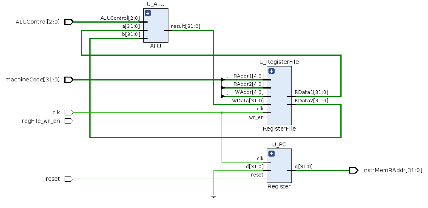
Instruction Memory 구현
`timescale 1ns / 1ps

// storing Machine Code
module InstructionMemory (  // only Read
    input logic [31:0] addr,

    output logic [31:0] data
);

    logic [31:0] rom[0:63];

    initial begin
        rom[0] = 31'h005201b3;  // add x6 x4 x5
        rom[1] = 31'h401184b3;  // sub x7 x2 x1 => 1
        rom[2] = 31'h0020f433;  // and x8 x1 x2 => 0
    end

    assign data = rom[addr[31:2]];
endmodule
rom[addr[31:2]] → 하위 2비트를 무시하는 이유
- 주소 크기
addr은 32비트 주소 입력rom은 32비트(4바이트) 크기의 요소 64개로 구성
- 4바이트 단위 접근
- ROM 배열의 각 요소는 32비트, 즉 4바이트
- 일반적으로 메모리는 바이트 단위로 주소를 할당
- 그러나 이 경우, 각 명령어가 4바이트(32비트)이기 때문에 주소를 4바이트 단위로 접근해야 함
- 주소 비트 시프트
addr[31:2]는 주소의 상위 30비트를 사용한다는 의미- 이는 주소를 4로 나누는 것과 같음
- 예를 들어, 주소가
32'h00000004이면, 이는 ROM 배열의 두 번째 요소를 가리킨다. 32'h00000004를 4로 나누면32'h00000001이 됩니다. 따라서rom[1]이 선택된다.
예시
- 주소가
32'h00000000인 경우addr[31:2]==32'h0000 0000 ~ 32'h0000 0003- 결과:
rom[0]선택
- 주소가
32'h00000004인 경우addr[31:2]==32'h0000 0004 ~ 32'h0000 0007- 결과:
rom[1]선택
- 주소가
32'h00000008인 경우addr[31:2]==32'h0000 0008 ~ 32'h0000 00011- 결과:
rom[2]선택

Control Unit 구현
`timescale 1ns / 1ps

module ControlUnit (  // only Read
    input logic [6:0] op,
    input logic [2:0] funct3,
    input logic [6:0] funct7,

    output logic       regFile_wr_en,
    output logic [2:0] ALUControl
);
    logic controls;

    assign regFile_wr_en = controls;

    always_comb begin
        case (op)
            7'b0110011: controls = 1'b1;  // R-Type
            7'b0000011: controls = 1'b0;  // IL-Type
            7'b0010011: controls = 1'b0;  // I-Type
            7'b0100011: controls = 1'b0;  // S-Type
            7'b1100011: controls = 1'b0;  // B-Type
            7'b0110111: controls = 1'b0;  // LUI-Type
            7'b0010111: controls = 1'b0;  // AUIPC-Type
            7'b1101111: controls = 1'b0;  // J-Type
            7'b1100111: controls = 1'b0;  // JI-Type
            default: controls = 1'b0;  // JI-Type
        endcase
    end

    always_comb begin
        case ({funct7[5], funct3})  // funct 값에 따라 ALU동작이 바뀜
            4'b0000: ALUControl = 3'b000; // add
            4'b1000: ALUControl = 3'b001; // sub
            4'b0110: ALUControl = 3'b011; // or
            4'b0111: ALUControl = 3'b010; // and
            default: ALUControl = 3'bx;
        endcase
    end

endmodule
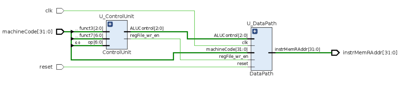
Core 구현
`timescale 1ns / 1ps


module CPU_Core (
    input logic        clk,
    input logic        reset,
    input logic [31:0] machineCode,

    output logic [31:0] instrMemRAddr
);

    logic w_regFile_wr_en;
    logic [2:0] w_ALUControl;

    ControlUnit U_ControlUnit (  // only Read
        .op(machineCode[6:0]),
        .funct3(machineCode[14:12]),
        .funct7(machineCode[31:25]),

        .regFile_wr_en(w_regFile_wr_en),
        .ALUControl(w_ALUControl)
    );

    DataPath U_DataPath (
        .clk(clk),
        .reset(reset),
        .machineCode(machineCode),
        .regFile_wr_en(w_regFile_wr_en),
        .ALUControl(w_ALUControl),

        .instrMemRAddr(instrMemRAddr)
    );
endmodule
top 구현
`timescale 1ns / 1ps

module RV32I (
    input logic clk,
    input logic reset
);

    logic [31:0] w_InstrMemAddr, w_InstrMemData;

    CPU_Core U_CPU_Core (
        .clk(clk),
        .reset(reset),
        .machineCode(w_InstrMemData),

        .instrMemRAddr(w_InstrMemAddr)
    );

    InstructionMemory U_ROM (  // only Read
        .addr(w_InstrMemAddr),

        .data(w_InstrMemData)
    );

endmodule
시뮬레이션
`timescale 1ns / 1ps

module tb_RV32I ();

    logic clk;
    logic reset;

    RV32I dut (
        .clk  (clk),
        .reset(reset)
    );

    always #5 clk = ~clk;

    initial begin
        clk   = 0;
        reset = 1'b1;
        #40 reset = 1'b0;
    end
endmodule
Machine Code 31'h00520333 == add x6 x4 x5 == 결과 9 정상 출력


왼쪽 사진 Program Counter에서 Address 32'b0를 전송(주소 포인터)하고
오른쪽 사진 Instruction Memory에서 해당 주소에 저장된 값(add X6 X4 X4 machine code)을 CPU_Core로 전송하여 프로세스를 진행한다.
3-1. 여러번 실행하기
- adder를 통해 Program Counter가 자동으로 증가하도록 설계
구현
Data Path Adder 추가
    Register U_PC (  // prgram counter
        .clk  (clk),
        .reset(reset),
        .d    (w_PC_Data),

        .q(instrMemRAddr)
    );

    adder U_Adder_ProgramCounter (
        .a(instrMemRAddr),
        .b(32'd4),

        .y(w_PC_Data)
    );
Program Counter Input으로 MUX를 추가
- PC의 출력(주소 포인터) 4씩 증가
- Instruction Memory 인덱스 1씩 증가(rom[0] → rom[1] → rom[2] → …)
- 위에서 설명했다시피 Address 4개가 하나의 레지스터를 가르키기 때문에 위와같이 인덱스는 1씩 증가한다.

시뮬레이션

Machine Code 31'h0020f433 == and x8 x1 x2 => 0 == 결과 0 정상 출력
아래 사이트를 이용하면 Machine Code를 간편하게 만들 수 있다!!

3-2. RV32I IL-Type Instruction
- RAM에 Access하기 위함!!
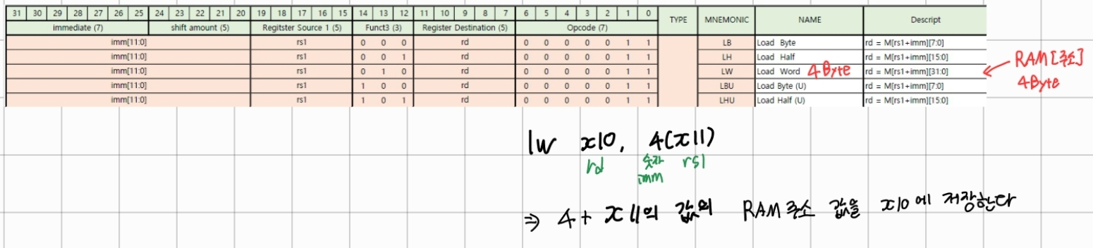
- ex) lw x10, x11, 4
- x11(Register File Read Data)와 imm값(상수)를 더한 값의 RAM 주소에 저장된 값을 x10에 저장한다.
- (4 + x11 데이터)를 포인터로 하여 해당 포인터가 가르키는 RAM 값을 가져와서 Register File에 저장한다.
- 4+x11 데이터 값이 RAM의 주소가 되는것!!!

Type RFWr_en AluSrcMuxSel RFWrtDataSrcMuxSel dataMem_wr_en
| Type | RFWr_en | AluSrcMuxSel | RFWrtDataSrcMuxSel | dataMem_wr_en |
| R | 1 | 0 | 0 | 0 |
| IL | 1 | 1 | 1 | 0 |
- 추가한 2개의 MUX에 0, 0 select 신호를 주면 R-Type Instruction을 사용할 수 있고 1, 1 select 신호를 주면 I-Type Instruction을 사용할 수 있다.
- Read Data1의 값과 imm값을 더한 값(ALU 덧셈 연산)을 RAM의 주소로 하여 해당 값을 읽는다.
`timescale 1ns / 1ps

module DataPath (
    input logic        clk,
    input logic        reset,
    input logic [31:0] machineCode,
    input logic        regFile_wr_en,
    input logic [ 2:0] ALUControl,
    input logic [31:0] dataMemRData,
    input logic        AluSrcMuxSel,
    input logic        RFWriteDataSrcMuxSel,

    output logic [31:0] instrMemRAddr,
    output logic [31:0] dataMemRAddr
);

    // logic [31:0] w_ALUResult, w_RegFileRData1, w_RegFileRData2, w_PC_Data;
    logic [31:0] w_RegFileRData1, w_RegFileRData2, w_PC_Data;
    logic [31:0] w_extendOut, w_AluSrcMuxOut, w_RFWirteDataSrcMuxOut;

    Register U_PC (  // prgram counter
        .clk  (clk),
        .reset(reset),
        .d    (w_PC_Data),

        .q(instrMemRAddr)
    );

    adder U_Adder_ProgramCounter (
        .a(instrMemRAddr),
        .b(32'd4),

        .y(w_PC_Data)
    );

    RegisterFile U_RegisterFile (
        .clk   (clk),
        .wr_en (regFile_wr_en),
        .RAddr1(machineCode[19:15]),
        .RAddr2(machineCode[24:20]),
        .WAddr (machineCode[11:7]),
        .WData (w_RFWirteDataSrcMuxOut),

        .RData1(w_RegFileRData1),
        .RData2(w_RegFileRData2)
    );

    mux_2x1 U_ALUSrcMux (
        .sel(AluSrcMuxSel),
        .a  (w_RegFileRData2),
        .b  (w_extendOut),

        .y(w_AluSrcMuxOut)
    );

    ALU U_ALU (
        .a         (w_RegFileRData1),
        .b         (w_AluSrcMuxOut),
        .ALUControl(ALUControl),

        .result(dataMemRAddr)
    );

    mux_2x1 U_RFWirteDataSrcMux (
        .sel(RFWriteDataSrcMuxSel),
        .a  (dataMemRAddr),
        .b  (dataMemRData),

        .y(w_RFWirteDataSrcMuxOut)
    );

    extend U_Extend (
        .instr(machineCode[31:7]),

        .immext(w_extendOut)
    );
endmodule


module RegisterFile (
    input logic        clk,
    input logic        wr_en,
    input logic [ 4:0] RAddr1,
    input logic [ 4:0] RAddr2,
    input logic [ 4:0] WAddr,
    input logic [31:0] WData,

    output logic [31:0] RData1,
    output logic [31:0] RData2
);
    logic [31:0] RegFile[0:31];  // 32bit 저장공간 32개

    initial begin  // 임의 초기값
        RegFile[0] = 32'd0;
        RegFile[1] = 32'd1;
        RegFile[2] = 32'd2;
        RegFile[3] = 32'd3;
        RegFile[4] = 32'd4;
        RegFile[5] = 32'd5;
    end

    always_ff @(posedge clk) begin
        if (wr_en) RegFile[WAddr] <= WData;
    end

    // address 0이면 0반환
    assign RData1 = (RAddr1 != 0) ? RegFile[RAddr1] : 0;
    assign RData2 = (RAddr2 != 0) ? RegFile[RAddr2] : 0;
endmodule


module Register (
    input logic        clk,
    input logic        reset,
    input logic [31:0] d,

    output logic [31:0] q
);

    always_ff @(posedge clk, posedge reset) begin : register  // Flip-Flop형태
        if (reset) begin
            q <= 0;
        end else begin
            q <= d;
        end
    end : register
    // : register -> 주석같은 느낌, 여기가 always문 끝이라는걸 나타냄, 없어도됨
endmodule


module ALU (
    input logic [31:0] a,
    input logic [31:0] b,
    input logic [ 2:0] ALUControl,

    output logic [31:0] result
);
    enum logic [2:0] {
        ADD = 3'b000,
        SUB = 3'b001,
        AND = 3'b010,
        OR  = 3'b011
    } alu_op_t;

    always_comb begin
        case (ALUControl)
            ADD:     result = a + b;
            SUB:     result = a - b;
            AND:     result = a & b;
            OR:      result = a | b;
            default: result = 32'bx;
        endcase
    end
endmodule


module adder (
    input logic [31:0] a,
    input logic [31:0] b,

    output logic [31:0] y
);
    assign y = a + b;
endmodule


// opcode제외 모든 신호 받아서
// imm bit(31:20)만 빼내고 이 신호를 32비트로 늘림
module extend (
    input logic [31:7] instr,

    output logic [31:0] immext
);
    assign immext = {{20{instr[31]}}, instr[31:20]};
    // sign bit(최상위 bit) 확장
    // 양수이면 0으로 확장되고 음수이면 1로 확장됨
endmodule


module mux_2x1 (
    input logic        sel,
    input logic [31:0] a,
    input logic [31:0] b,

    output logic [31:0] y
);
    always_comb begin
        case (sel)
            1'b0: y = a;
            1'b1: y = b;
            default: y = 32'bx;
        endcase
    end
endmodule`timescale 1ns / 1ps
module ControlUnit ( // only Read
input logic [6:0] op,
input logic [2:0] funct3,
input logic [6:0] funct7,
output logic regFile_wr_en,
output logic AluSrcMuxSel,
output logic RFWriteDataSrcMuxSel,
output logic dataMem_wr_en,
output logic [2:0] ALUControl
);
logic [5:0] controls;
logic [1:0] w_AluOp;
assign {regFile_wr_en, AluSrcMuxSel, RFWriteDataSrcMuxSel, dataMem_wr_en, w_AluOp} = controls;
always_comb begin
case (op)
// regFile_wr_en, AluSrcMuxSel, RFWriteDataSrcMuxSel, dataMem_wr_en, ALUOp
7'b0110011: controls = 6'b1_0_0_0_10; // R-Type
7'b0000011: controls = 6'b1_1_1_0_00; // IL-Type
7'b0010011: controls = 6'b0; // I-Type
7'b0100011: controls = 6'b0; // S-Type
7'b1100011: controls = 6'b0; // B-Type
7'b0110111: controls = 6'b0; // LUI-Type
7'b0010111: controls = 6'b0; // AUIPC-Type
7'b1101111: controls = 6'b0; // J-Type
7'b1100111: controls = 6'b0; // JI-Type
default: controls = 6'b0; // JI-Type
endcase
end
always_comb begin
case (w_AluOp)
2'b00: ALUControl = 3'b000; // add
2'b01: ALUControl = 3'b001; // sub
default: begin
case (funct3) // R-Type, I-Type ALU
3'b000: begin
if (funct7[5] & op[5]) ALUControl = 3'b001; // sub
else ALUControl = 3'b000; // add
// R-Type add와 sub가 funct3가 같기에 funct7으로 판단
end
3'b010: ALUControl = 3'b000; // slt
3'b110: ALUControl = 3'b011; // or
3'b111: ALUControl = 3'b010; // and
default: ALUControl = 3'bx;
endcase
end
endcase
end
endmodule
`timescale 1ns / 1ps

module DataMemory (
    input logic        clk,
    input logic        wr_en,
    input logic [31:0] addr,
    input logic [31:0] wdata,

    output logic [31:0] rdata
);
    logic [31:0] ram[0:63];

    initial begin
        int i;
        for (i = 0; i < 64; i++) begin
            ram[i] = 100 + i;
        end
    end
    assign rdata = ram[addr[31:2]];

    always_ff @(posedge clk) begin
        if (wr_en) ram[addr[31:2]] <= wdata;
    end
endmodule
시뮬레이션
    initial begin
        rom[0] = 32'h00520333;  // add x6, x4, x5
        rom[1] = 32'h401184b3;  // sub x9, x3, x2 => 1
        rom[2] = 32'h00602503;  // lw x10, x0, 6
        rom[3] = 32'h00a02583;  // lw x11, x0, 10
    end
위와 같은 Machine Code 실행
123
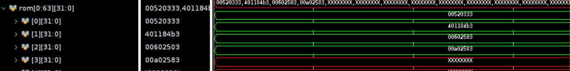
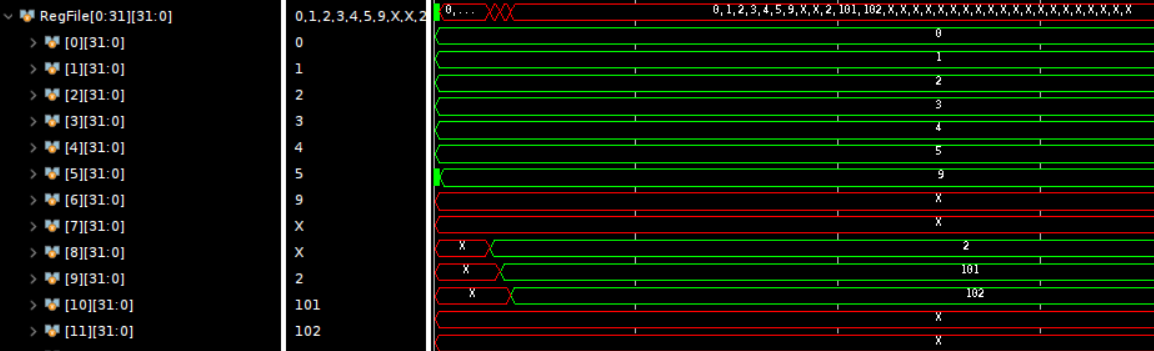

- ROM : Machine Code가 저장되어 있다.
- Register File : RAM에서 읽은 값(Reg[10] → 101)이 저장되어 있다.
- RAM : 100부터 1씩 증가되는 값이 임의로 저장되어 있다.
Made By Minseok KIM
'VerilogHDL > Study' 카테고리의 다른 글
| [VerilogHDL] AXI-Lite 구현 (0) | 2024.06.18 |
|---|---|
| [VerilogHDL] CPU 기본 구조, 메모리, Counter 설계(Control Unit, Data Path) (1) | 2024.06.03 |
| [VerilogHDL] FIFO, UART&FIFO (0) | 2024.05.30 |
| [VerilogHDL] Verification(32bit register, BRAM) (0) | 2024.05.23 |
| [VerilogHDL] System Verilog 기초 (0) | 2024.05.22 |
Let's Be Happy!
도움이 되었으면 좋겠어요 :)
![[VerilogHDL] AXI-Lite 구현](https://img1.daumcdn.net/thumb/R750x0/?scode=mtistory2&fname=https%3A%2F%2Fblog.kakaocdn.net%2Fdna%2FbmypW7%2FbtsH3QmndVl%2FAAAAAAAAAAAAAAAAAAAAAOcAKloXAwvhb2Kn-Ayj86Qq9eutpiJOQzoHe2_U1jBg%2Fimg.png%3Fcredential%3DyqXZFxpELC7KVnFOS48ylbz2pIh7yKj8%26expires%3D1777561199%26allow_ip%3D%26allow_referer%3D%26signature%3DjHt8VA2kIjll7WchW46DFxWAxUE%253D)
![[VerilogHDL] CPU 기본 구조, 메모리, Counter 설계(Control Unit, Data Path)](https://img1.daumcdn.net/thumb/R750x0/?scode=mtistory2&fname=https%3A%2F%2Fblog.kakaocdn.net%2Fdna%2FrzOB9%2FbtsHL7P7B17%2FAAAAAAAAAAAAAAAAAAAAAMc-QWDRhT_hzPR7x7Y9i-Pcn8pTNy7-UukWGXEzN8Wy%2Fimg.png%3Fcredential%3DyqXZFxpELC7KVnFOS48ylbz2pIh7yKj8%26expires%3D1777561199%26allow_ip%3D%26allow_referer%3D%26signature%3DsE7yL6Eo2HZlbfsgQ%252FXyXkURY5o%253D)
![[VerilogHDL] FIFO, UART&FIFO](https://img1.daumcdn.net/thumb/R750x0/?scode=mtistory2&fname=https%3A%2F%2Fblog.kakaocdn.net%2Fdna%2FppB3S%2FbtsHHS6e5x6%2FAAAAAAAAAAAAAAAAAAAAAM3nqxC-Nf1P9Z24uueWrVDX6_3B_gF2Lu2vSjaIhBGv%2Fimg.png%3Fcredential%3DyqXZFxpELC7KVnFOS48ylbz2pIh7yKj8%26expires%3D1777561199%26allow_ip%3D%26allow_referer%3D%26signature%3D5kG2yrKN4oOl2hPaed%252Fx5hT%252BgeE%253D)
![[VerilogHDL] Verification(32bit register, BRAM)](https://img1.daumcdn.net/thumb/R750x0/?scode=mtistory2&fname=https%3A%2F%2Fblog.kakaocdn.net%2Fdna%2Fcth4gF%2FbtsHyFT7n8o%2FAAAAAAAAAAAAAAAAAAAAAHSK9Mf3bSeiTIhNY2OZ_mKPS_jQQ7UEHib1rJqQ0IEx%2Fimg.png%3Fcredential%3DyqXZFxpELC7KVnFOS48ylbz2pIh7yKj8%26expires%3D1777561199%26allow_ip%3D%26allow_referer%3D%26signature%3DTxP5OIRq1G2flv%252FpJl9WghM3jaQ%253D)