![[VerilogHDL] 반도체 칩 설계과정, Vivado 시작하기, 시뮬레이션, Logic Gates](https://img1.daumcdn.net/thumb/R750x0/?scode=mtistory2&fname=https%3A%2F%2Fblog.kakaocdn.net%2Fdn%2FblsNK0%2FbtsHkkuXN0w%2FhBXxnbJZ5tQdfW1BvKVdlk%2Fimg.png)

[VerilogHDL] 반도체 칩 설계과정, Vivado 시작하기, 시뮬레이션, Logic GatesVerilogHDL/Study2024. 5. 9. 01:00
Table of Contents
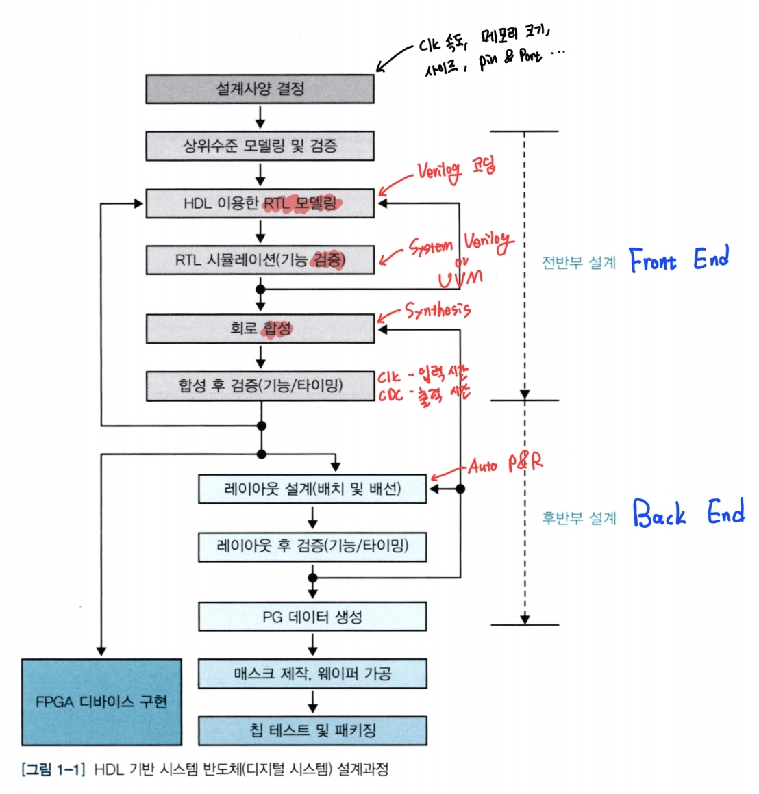
1. 반도체 칩 설계 과정
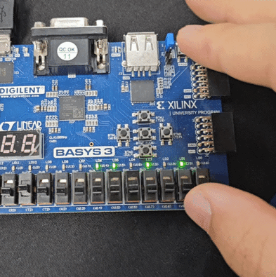
2. Basys3 FPGA Board
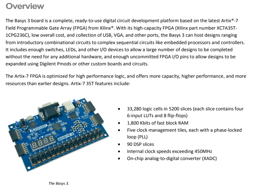
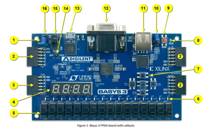
- 가운데 칩이 FPGA Chip(ARTIX-7 (XC7A35T-CPG236C))
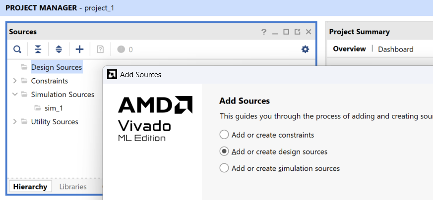
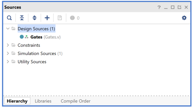
파일 만들기
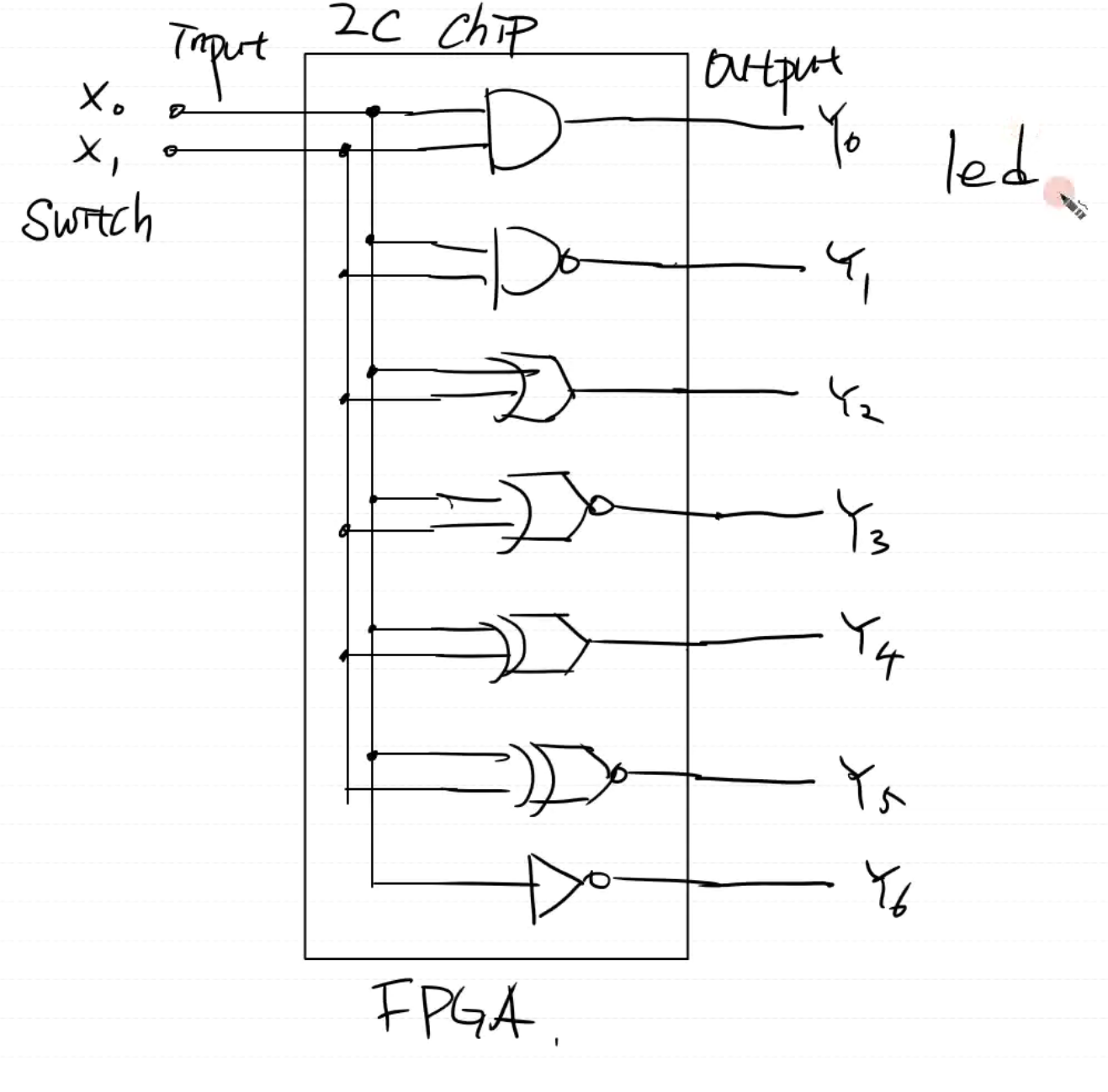
3. 로직 게이트 설계하기
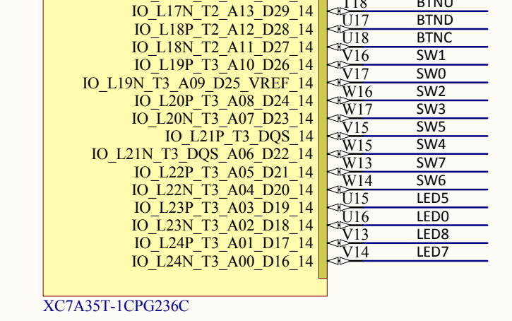
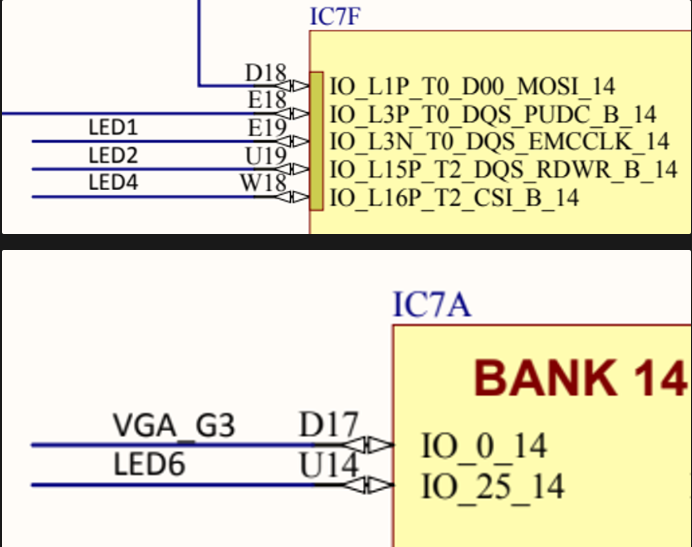
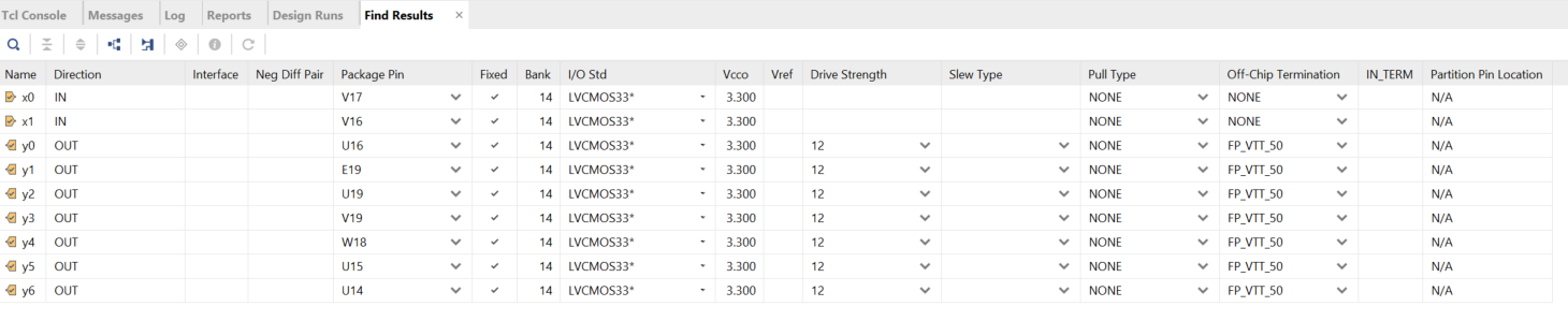
위와 같이 Datasheet에 각 핀에 연결된 HW가 표기되어 있다.
SW0 : V17, SW1 : V16
LED0 : U16, LED1 : E19, …
설계 과정
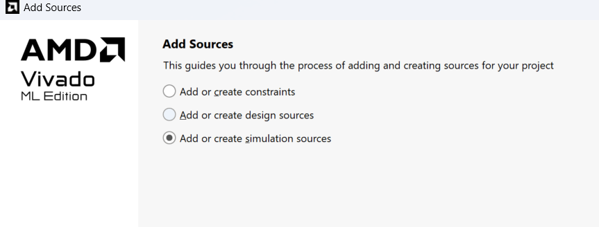
1. Design Source 작성
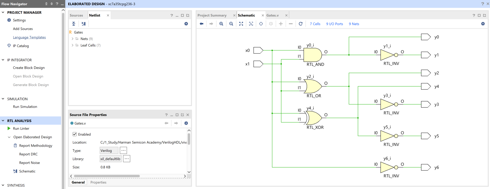
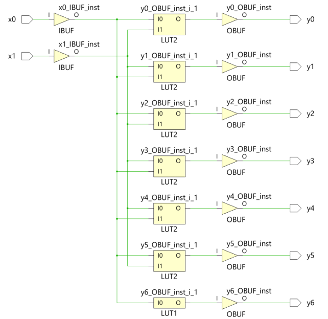
2. RTL Schematic 확인 & IO Port 설정
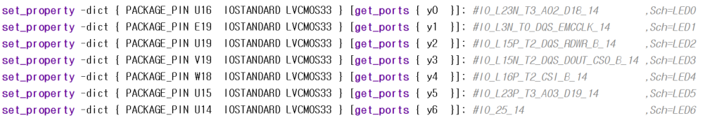
IO 포트 설정을 위와같이 코드로 작성할 수 있음
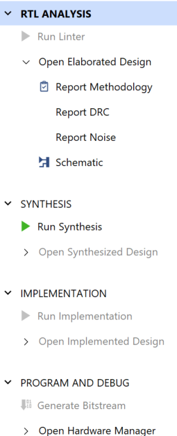
3. Synthesis → Implementation → Program And Debug 순서로 실행
- Synthesis(합성) : Verilog code(논리) → HW(물리)로 바꾸는 과정
- 이 과정에서 Hardware Netlist가 생성됨
- RTL schematic과는 다른 Synthesis schematic netlist가 만들어 진다.(FPGA에 적합한 netlist 생성)
- Implement(구현) : FPGA에 맞는 배치, 회로
- 실제 FPGA에 어떻게 배치할 것인지 Bitstream 파일을 생성
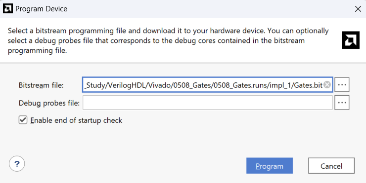
4. Program Device → 위와 같은 창에서 Program 클릭 → 프로그램 업로드
- Bitstream 파일을 FPGA에 업로드하는 과정
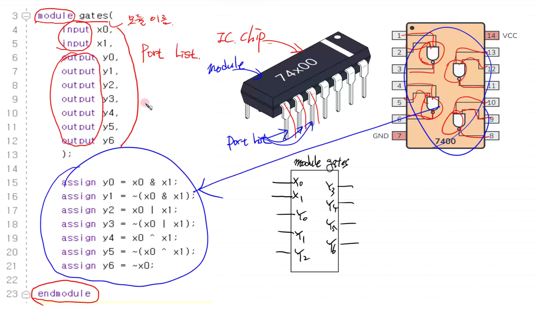
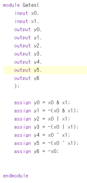
- `Module gates` : 모듈 이름
- `input, output` : Port list
- `assign` : 모듈 안의 회로
4. Verilog 문법
- assign문 : 이용한 Continous Assignment 연속 할당문
- `assign y0 = x0 & x1`
- y0 : 출력 / X0, X1 : 입력 / & : AND 회로 / = : 연결한다
- x0와 x1을 AND 게이트 입력으로 넣고 그 출력을 y0와 연결한다.
- primitive : 회로 이용(Gate 회로 이용)
- AND, OR 같은 기본 디지털 회로 정의
module Gates( input x0, input x1, output y0, output y1, output y2, output y3, output y4, output y5, output y6 ); // assign y0 = x0 & x1; // assign y1 = ~(x0 & x1); // assign y2 = x0 | x1; // assign y3 = ~(x0 | x1); // assign y4 = x0 ^ x1; // assign y5 = ~(x0 ^ x1); // assign y6 = ~x0; // Gate Primitive and(y0, x0, x1); nand(y1, x0, x1); or(y2, x0, x1); nor(y3, x0, x1); xor(y4, x0, x1); xnor(y5, x0, x1); not(y6, x0); endmodule - always문(조건이 만족되는 동안 동작 수행) : 논리, 행위수준 모델링
- 블록 내에서 특정한 이벤트나 조건이 발생할 때마다 블록 내의 명령문 실행
- ex) 클럭 rising edge마다 실행
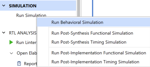
5. Simualtion
- 시뮬레이션 과정
- 시뮬레이션 코드
module tb_Gates();

    reg x0;
    reg x1;
    wire y0;
    wire y1;
    wire y2;
    wire y3;
    wire y4;
    wire y5;
    wire y6;

    Gates test_bench(
      .x0(x0),
      .x1(x1),
      .y0(y0),
      .y1(y1),
      .y2(y2),
      .y3(y3),
      .y4(y4),
      .y5(y5),
      .y6(y6)
    );

    initial begin
       #00 x1 = 0; x0 = 0;
       #10 x1 = 0; x0 = 1;
       #10 x1 = 1; x0 = 0;
       #10 x1 = 1; x0 = 1;
       #10 $finish;
    end


endmodule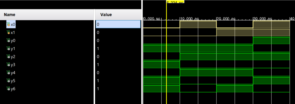
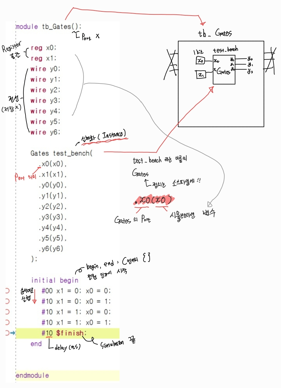
- `module tb_Gates()`는 Simualtion용이기에 Port 없음
- input 변수 : `reg` ← Register 공간 할당
- ouput 변수 : `wire` ← 전선 연결
- `Gates test_bench` : test_bench라는 IC는 Gates의 종속 (실체화)
- 논리 구조를 Gates module을 따라감
- `.x0` : 부모 클래스(Gates)의 Port
- `.x0(x0)` : Gates의 x0 Port와 x0 변수를 연결해준다 라는 의미 (x0는 reg input으로 선언되어 있음)
- `initial begin ~ end` : 시뮬레이션 하고자 하는 input을 입력해주면 된다.
- #10 : ns delay
Made By Minseok KIM
'VerilogHDL > Study' 카테고리의 다른 글
| [VerilogHDL] FSM 코딩(Moore, Mealy) - 버튼, UpCounter (0) | 2024.05.19 |
|---|---|
| [VerilogHDL] 조합 논리 회로 & 순차 논리 회로, Latch & FlipFlop (0) | 2024.05.19 |
| [VerilogHDL] C&Verilog차이, SystemVerilog 기본, 8bit Adder FND, 만진 카운터 (0) | 2024.05.16 |
| [VerilogHDL] System Verilog, 4bit Adder FND 출력 (0) | 2024.05.16 |
| [VerilogHDL] HalfAdder, FullAdder, 4bit Adder (0) | 2024.05.09 |
@민바Minba :: Minba's blog
Let's Be Happy!
도움이 되었으면 좋겠어요 :)
![[VerilogHDL] 조합 논리 회로 & 순차 논리 회로, Latch & FlipFlop](https://img1.daumcdn.net/thumb/R750x0/?scode=mtistory2&fname=https%3A%2F%2Fblog.kakaocdn.net%2Fdn%2FSF2r6%2FbtsHtOdeWqq%2Fj9KnstjOc4HKyuyYtH1lA0%2Fimg.png)
![[VerilogHDL] C&Verilog차이, SystemVerilog 기본, 8bit Adder FND, 만진 카운터](https://img1.daumcdn.net/thumb/R750x0/?scode=mtistory2&fname=https%3A%2F%2Fblog.kakaocdn.net%2Fdn%2FHWO9v%2FbtsHqbzgbYD%2FUAoHdNYYi9zPTYOsETtu81%2Fimg.png)
![[VerilogHDL] System Verilog, 4bit Adder FND 출력](https://img1.daumcdn.net/thumb/R750x0/?scode=mtistory2&fname=https%3A%2F%2Fblog.kakaocdn.net%2Fdn%2FbpRigX%2FbtsHp32iq76%2FekHf18H6oq2HZElY9OjyTk%2Fimg.png)
![[VerilogHDL] HalfAdder, FullAdder, 4bit Adder](https://img1.daumcdn.net/thumb/R750x0/?scode=mtistory2&fname=https%3A%2F%2Fblog.kakaocdn.net%2Fdn%2F4bG43%2FbtsHgDiRNvy%2FkKVghAr98ONRN3kiFtyGo1%2Fimg.png)